-
Alkane Indium_tin_oxide YttriaStabilizedZirconia Insulator Holes align Deposition molecular_self_assembly Solar Treatment Electical&Electronics PinpointPFM dielectric_trench light_emission Change Polydimethylsiloxane CalciumHydroxide cannabinoid Ca10(PO4)6(OH)2 Scratch light_emitting optoelectronics Monisha lithography Zhi CaMnO3 BlockCopolymer fluoroalkane Heat CuParticle Dental DOE Memory Nanostructure AAO
Report image
If you found this image unacceptable, please let us know. We will review your report and take action if we determine this image is really unacceptable.
MoS2 Layers on SiO2
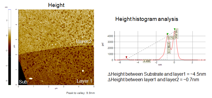
Scanning Conditions
- System: NX10
- Scan Mode: Non-contact
- Cantilever: AC160TS (k=26N/m, f=300kHz)
- Scan Size: 5μm×5μm
- Scan Rate: 1Hz
- Pixel Size: 256 × 256
- Scan Mode: Non-contact
- Cantilever: AC160TS (k=26N/m, f=300kHz)
- Scan Size: 5μm×5μm
- Scan Rate: 1Hz
- Pixel Size: 256 × 256