-
GaN Yttria_stabilized_Zirconia Electronics Semiconductor ForceMapping ScanningTunnelingMicroscopy Transparent UnivMaryland IRDetector Global_Comm conductive CP-AFM Edwin VortexCore DIWafer Potential FailureAnalysis InLiquid Hole Molybdenum Scratch aluminum_nitride MfmAmplitude ContactModeDot PtfeFilter ForceDistanceSpectroscopy Zagreb Worcester_Polytechnic_Institute Mapping Bacteria Aluminum Fujian Led Ferrite TiO2
Report image
If you found this image unacceptable, please let us know. We will review your report and take action if we determine this image is really unacceptable.
Monolayer Graphene on PDMS Surface
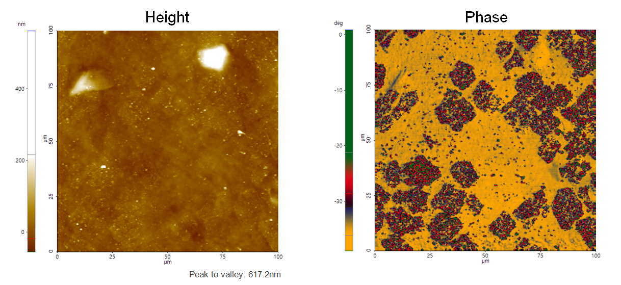
Monolayer Graphene grown on Cu foil using CVD process is transferred on to PDMS substrate.
Scanning Conditions
- System: NX20
- Scan Mode: Tapping
- Cantilever: Access-NC (k=113N/m, f=330kHz)
- Scan Size: 100μm×100μm
- Scan Rate: 0.6Hz
- Pixel Size: 256 × 256
- Scan Mode: Tapping
- Cantilever: Access-NC (k=113N/m, f=330kHz)
- Scan Size: 100μm×100μm
- Scan Rate: 0.6Hz
- Pixel Size: 256 × 256