-
Wafer Polyaniline SrO Beads Leakage AtomicLayer MLCC SingleCrystal Hysteresys HexagonalBoronNitride LiquidCell temperature controller AFM Treatment AIN lithography HumanHair BiFeO3 BTO ForceDistanceSpectroscopy non_contact Sic CP-AFM ForceVolumeImage InsulatorFilm MechanicalProperty Silicon SFAs SmalScan Magnetic Force Microscopy CancerCell ImideMonomer MetalCompound ContactModeDots Inorganic_Compound AmplitudeModulation
Report image
If you found this image unacceptable, please let us know. We will review your report and take action if we determine this image is really unacceptable.
MoS2 Layers on SiO2
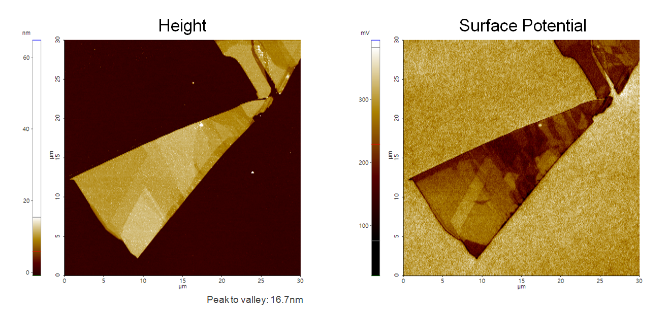
A few layers of MoS2 on SiO2
Scanning Conditions
- System: NX10
- Scan Mode: AM-KPFM
- Cantilever: NSC36Cr-Au B (k=2N/m, f=130kHz)
- Scan Size: 30μm×30μm
- Scan Rate: 0.3Hz
- Pixel Size: 512 × 256
- Scan Mode: AM-KPFM
- Cantilever: NSC36Cr-Au B (k=2N/m, f=130kHz)
- Scan Size: 30μm×30μm
- Scan Rate: 0.3Hz
- Pixel Size: 512 × 256