-
SelfAssembly Celebration FailureAnalysis YszSubstrate molecular_beam Wafer PvdfFilm mfm_amplitude mechanical property BCZT TemperatureControllerAFM Electrical&Electronics small_scan Monisha ContactModeDots Indium_tin_oxide AnodizedAluminumOxide vertical_PFM Spincast Al2O3 ScratchMode self-assembly C_AFM Thermal Gold light_emitting Microchannel Stiffness TPU Conductivity Laser Cross-section Hexylthiophene Array HanyangUniv
Report image
If you found this image unacceptable, please let us know. We will review your report and take action if we determine this image is really unacceptable.
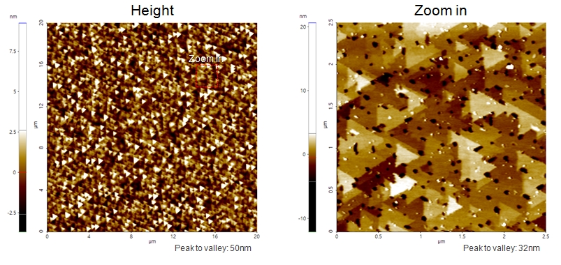
LiNbO3 wafer
Scanning Conditions
- System: NX10
- Scan Mode: Non-contact
- Cantilever: AC55TS (k=85N/m, f=1600kHz)
- Scan Size:20μm×20μm, 2.5μm×2.5μm
- Scan Rate: 5Hz, 10Hz
- Pixel: 512×512, 256×256
- Scan Mode: Non-contact
- Cantilever: AC55TS (k=85N/m, f=1600kHz)
- Scan Size:20μm×20μm, 2.5μm×2.5μm
- Scan Rate: 5Hz, 10Hz
- Pixel: 512×512, 256×256