-
MolybdenumDisulfide InsulatorFilm Growth Polyethylene NUS_NNI_Nanocore Ptfe vertical_PFM ULCA VerticalPFM Conductive AFM Conductance AIN AtomicLayer hard_disk_media ContactMode Nanotechnology WS2 Optoelectonics Ca10(PO4)6(OH)2 FAFailureAnlaysis MeltingPoint Zagreb solar_cell Patterns AM_SKPM Hexylthiophene PDMS Pores Perovskite Cell DOE Blood CopperFoil Litho Ram
Report image
If you found this image unacceptable, please let us know. We will review your report and take action if we determine this image is really unacceptable.
Polymer patterns on Si (1/2)
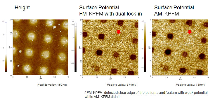
Scanning Conditions
- System: NX10
- Scan Mode: KPFM
- Cantilever: NSC36Cr-Au (k=1N/m, f=90kHz)
- Scan Size: 10μm×10μm
- Scan Rate: 0.2Hz
- Pixel: 512×256