-
Current OrganicSemiconductor HfO2 Molybdenum_disulfide atomic_layer Scratch cooling StainlessSteel H-BN StyreneBeads Laser OpticalWaveguides cannabidiol Vinylpyridine PetruPoni_Institute Hole Bismuth Tungsten Pores EPFL Array TungstenThinFilmDeposition Scanning_Thermal_Microscopy LateralForce Galfenol Piezo doped Lattice Graphene StrontiumTitanate Domain Al2O3 Mechanical&nanotechnology CuSubstrate Sperm
Report image
If you found this image unacceptable, please let us know. We will review your report and take action if we determine this image is really unacceptable.
Taegeuk Mark Lithography on PZT
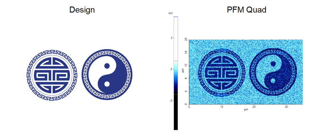
Re-arranged the domain pole direction on PZT surface using bias mode of lithography.
Scanning Conditions
- System: NX10
- Scan Mode: Lithography
- Cantilever: PPP-ContScPt (k=0.2N/m, f=25kHz)
- Scan Size: 35μm×20μm
- Scan Rate: 0.5Hz
- Pixel Size: 1024 × 1024
- Tip Bias: 10V for patterned area
- Scan Mode: Lithography
- Cantilever: PPP-ContScPt (k=0.2N/m, f=25kHz)
- Scan Size: 35μm×20μm
- Scan Rate: 0.5Hz
- Pixel Size: 1024 × 1024
- Tip Bias: 10V for patterned area