-
MonoLayer Yttria_stabilized_Zirconia INSPParis PtfeMembrane UnivCollegeLondon Gold CopperFoil PrCurve NtuEee Polydimethylsiloxane ULCA Ceramic light_emitting Dopped Topography Lanthanum_aluminate suspended_graphene MechanicalProperties self_healing FailureAnalysis temperature controller AFM Etch SicMosfet semifluorinated alkane CrossSection Electical&Electronics Ferroelectric OpticalModulator contact CalciumHydroxyapatite multi_layer Techcomp Annealed SurfaceChange Array
Report image
If you found this image unacceptable, please let us know. We will review your report and take action if we determine this image is really unacceptable.
ITO Film Sputter Deposited onto Silicon
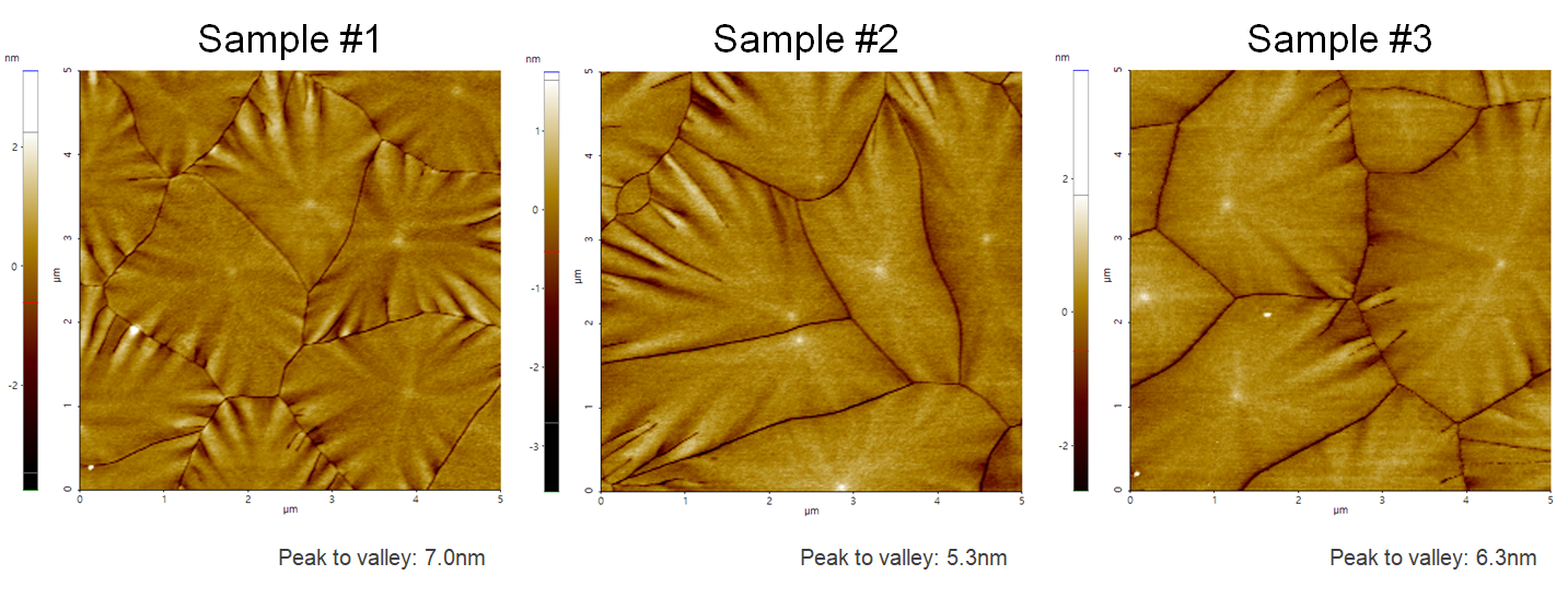
ITO-film, which was sputter deposited onto silicon. The grain size of those samples was influenced by changing the process settings in the Cluterline RAD sputter deposition system, one of the deposition tool platforms manufactured by Evatec.
Scanning Conditions
- System: NX10
- Scan Mode: Non-contact
- Cantilever: PPP-EFM (k=2.8N/m, f=75kHz)
- Scan Size: 5μm×5μm
- Scan Rate: 0.1Hz
- Pixel Size: 256 × 256
- Scan Mode: Non-contact
- Cantilever: PPP-EFM (k=2.8N/m, f=75kHz)
- Scan Size: 5μm×5μm
- Scan Rate: 0.1Hz
- Pixel Size: 256 × 256